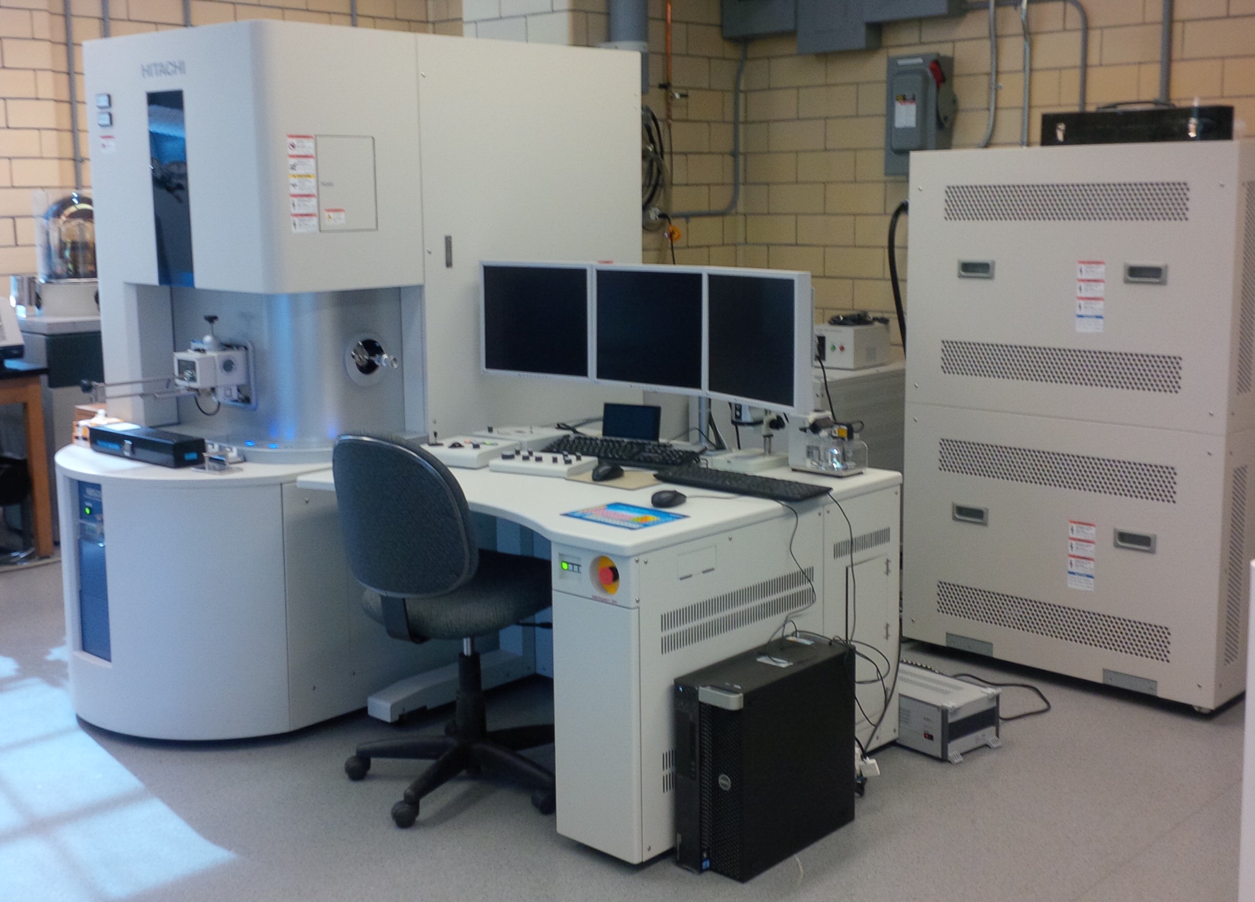
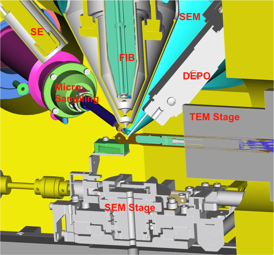
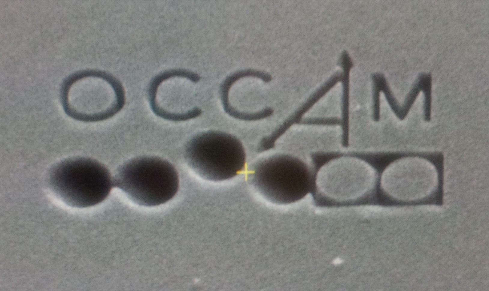
Allows for site-specific analysis, deposition, and removal of material in the micron and submicron range.
- Ultrahigh performance FIB
- Ga FIB optics
- > 50 nA max. beam current at 40kV
- Integrated Micro-sampling system
- Fully integrated lift-out system
- Absorbed current imaging
- High precision end-point detection
- Mill & Monitor
- Section-view
- Live Fabrication
- High Resolution SEM
- 1.5 nm @ 5kV, at Cross-point
- 1.0 nm @ 15kV, at Cross-point
- 0.8 nm @ 30kV, at Cross-point
- Holders compatible with TEM/STEM
|
 i-beam:
40-2.0 kV, <5nm spot size
(+) machine/deposit
(-) implantation/damage (not ideal for imaging)
e-beam:
30-0.5kV, 0.8nm spot size
(+) no implantation/damage (ideal for imaging)
(-) slow machining/deposition
e-beam + i-beam = dual beam
i-beam is 58 deg. from e-beam
(+) e-beam images of the FIB prepared cross-section face without moving the stage!
(+) serial sectioning for 3D info. = “slice + view”
(-) very complicated/expensive
|
“Creating partnerships for innovative research”
Open Centre for the Characterisation of Advanced Materials
